
Smart Manufacturing for Semiconductors: Where AI Inspection and MES Deliver Measurable Gains





Where smart manufacturing for semiconductors starts to show real value
Smart manufacturing for semiconductors matters when yield pressure, process variation, and response time begin to collide on the same line.
The measurable gains usually appear where AI inspection and MES are connected, not treated as separate digital projects.
In practical terms, that means defect signals are captured earlier, production context is clearer, and traceability becomes useful instead of merely archived.
For an industrial intelligence platform like GPTWM, this matters beyond semiconductors alone.
Its focus on metrology, tooling precision, and the last mile of manufacturing makes smart manufacturing for semiconductors a natural reference point for broader factory modernization.
The lesson is consistent across industries: precision data only becomes operational value when it is tied to process decisions.
Why the same architecture works differently across semiconductor operations
Different semiconductor environments do not ask the same questions of AI inspection or MES.
A front-end wafer fab focuses on microscopic defects, process drift, and equipment correlation.
An assembly and packaging site often cares more about throughput stability, bonding quality, and lot genealogy across multiple workstations.
The inspection model, data granularity, and MES workflow therefore need different priorities.
That is where many digital programs lose momentum.
They deploy a generic smart manufacturing for semiconductors stack, then wonder why one site improves quickly while another only gains dashboard visibility.
A better starting point is to judge each scenario by three conditions: defect cost, decision speed, and traceability depth.
Front-end production: small defects, large financial impact
In wafer fabrication, one classification error can distort downstream analysis for an entire lot.
Here, smart manufacturing for semiconductors depends on AI inspection that can separate nuisance signals from yield-relevant anomalies.
MES adds value by tying inspection outcomes to recipes, chamber history, operator actions, and rework status.
Without that connection, image intelligence remains isolated and root cause analysis stays slow.
More advanced sites also use MES context to trigger sampling changes after excursions, which reduces blind spots without overloading metrology tools.
Back-end lines: speed matters, but only with controlled variation
Packaging and final test present a different balance.
Cycle time is under constant pressure, while defect patterns often involve bonding, placement, marking, or handling variation.
In this setting, smart manufacturing for semiconductors works best when AI inspection supports line pacing instead of slowing it down.
MES should help isolate which equipment combination, material batch, or shift condition changed first.
The goal is less about collecting every image forever, and more about linking the right evidence to the right production event.
The common scenarios that reveal whether AI inspection and MES are well matched
In actual deployment, a few scenarios quickly expose whether the architecture fits the plant or merely looks modern on paper.
- Frequent false alarms during optical inspection usually indicate weak model tuning or missing MES context.
- Slow disposition of suspect lots often points to fragmented genealogy and poor event mapping.
- Stable throughput with unstable yield suggests inspection is catching symptoms, not process causes.
- High traceability effort with low analytical value means data capture is broad, but not structured for decisions.
These signals matter because smart manufacturing for semiconductors is not defined by how much data is stored.
It is defined by whether the factory can act earlier and with more confidence.
Different scenarios need different decision rules
The differences become clearer when process environments are compared side by side.
This is why smart manufacturing for semiconductors should be assessed by operational fit, not only software capability lists.
What often gets misjudged before implementation
One common mistake is assuming better inspection accuracy alone will improve yield.
If MES cannot map inspection results to process states, the line may identify more defects while learning very little.
Another mistake is treating similar lines as identical environments.
Differences in material flow, tool age, maintenance discipline, and handoff rules can change what smart manufacturing for semiconductors needs to prioritize.
There is also a recurring cost error.
Projects are judged by acquisition cost, while integration effort, model retraining, and data governance are underestimated.
GPTWM’s broader view across metrology, industrial tooling, and digital factory transitions is useful here.
It highlights a familiar industrial pattern: precision systems succeed when measurement logic, equipment behavior, and workflow control are designed together.
A practical way to match the solution to the site
A workable evaluation sequence is usually more valuable than a large transformation blueprint.
- Map where yield loss, delay, or rework starts to accelerate rather than where data is easiest to collect.
- Check whether defect images can be linked to lot history, equipment states, and operator events in near real time.
- Define which decisions must be automated, which need review, and which only need better visibility.
- Set retraining rules for AI inspection based on product mix shifts, not calendar dates alone.
- Measure performance through scrap avoided, response time reduced, and containment accuracy improved.
This keeps smart manufacturing for semiconductors grounded in plant economics and execution discipline.
Why this matters beyond a single fab
Semiconductor operations are often the sharpest test case for digital manufacturing because tolerance is tight and error costs are immediate.
That is also why the topic resonates with GPTWM’s mission.
Its Strategic Intelligence Center follows how precision tools, metrology discipline, and intelligent control reshape industrial performance across sectors.
In that broader context, smart manufacturing for semiconductors is not an isolated niche.
It is a leading indicator of how factories convert high-precision data into process confidence.
The next step is straightforward: identify the operating scenario, compare traceability depth with defect cost, and test whether AI inspection and MES are solving the same production problem.
That comparison usually reveals where measurable gains are realistic, where integration work is still missing, and where deployment should begin first.
Related News
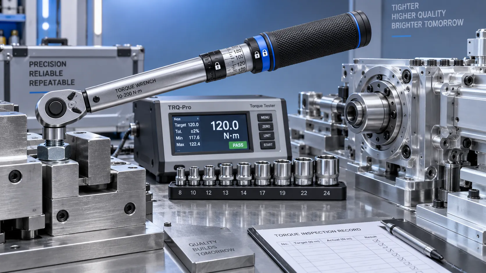
Selecting Adjustable Torque Tools for Repeatable Fastener Assembly
Adjustable torque tools: learn how to match range, accuracy, control methods, calibration, and ergonomics for repeatable, reliable fastener assembly.
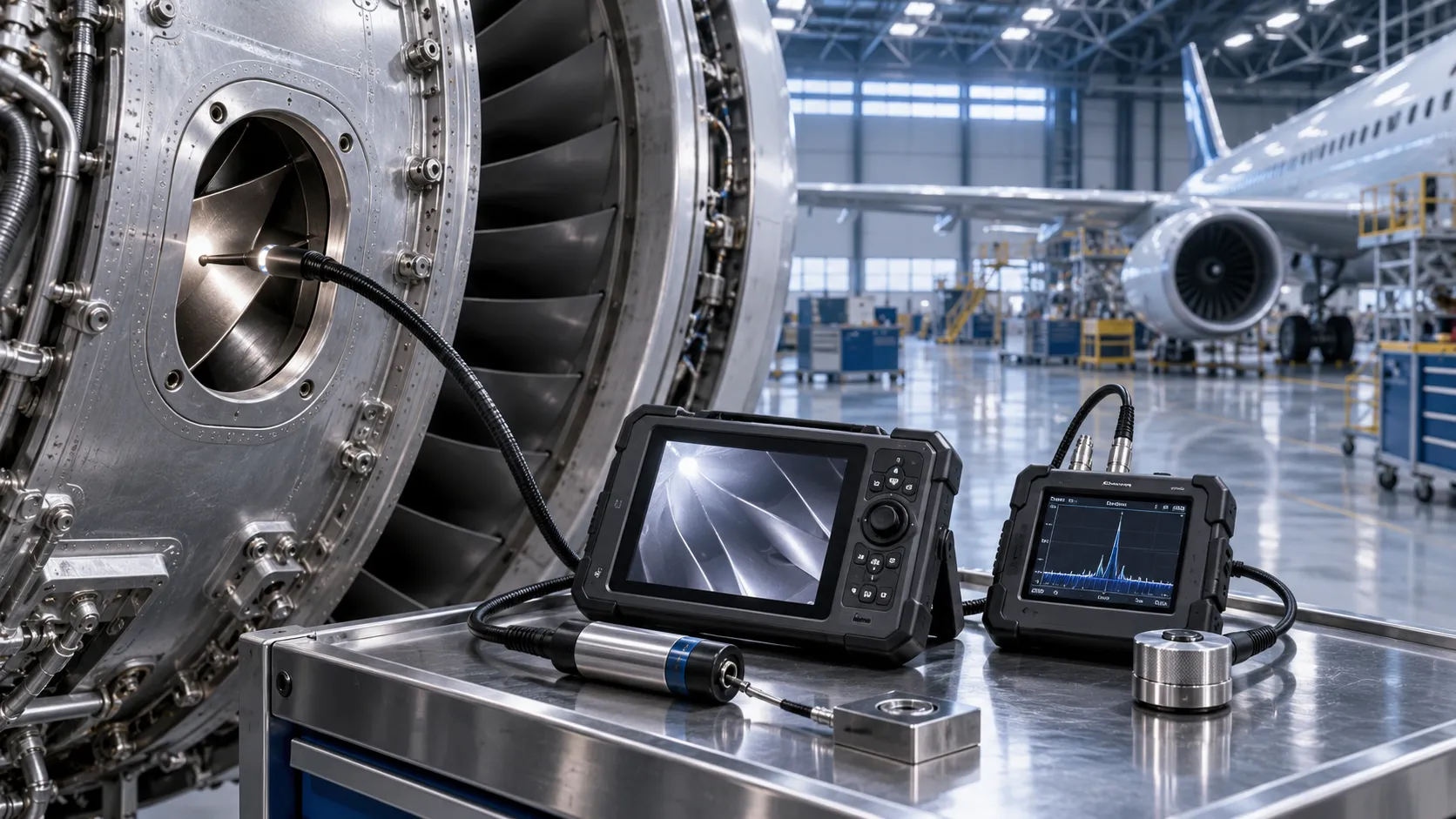
How to Select Aerospace Inspection Tools for Aircraft Maintenance Tasks
Aerospace maintenance inspection tools: learn how to select reliable, traceable equipment for aircraft access, accuracy, calibration, and compliant maintenance decisions.
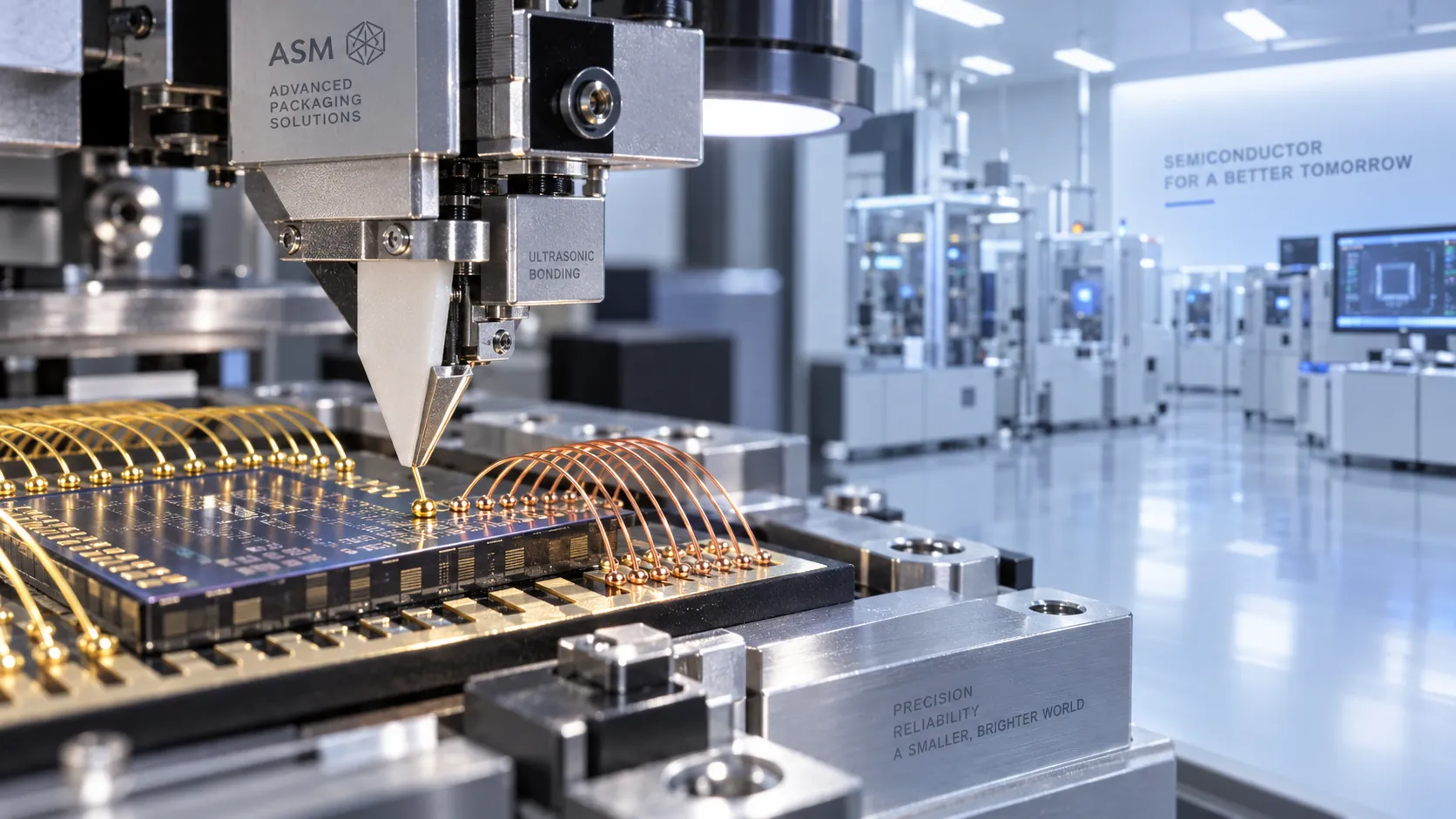
How to Select Wire Bonding Tools for Fine-Pitch Semiconductor Packaging
Explore semiconductor manufacturing tools for wire bonding and learn how to select precision solutions for fine-pitch packaging, reliable loops, accuracy, and yield.
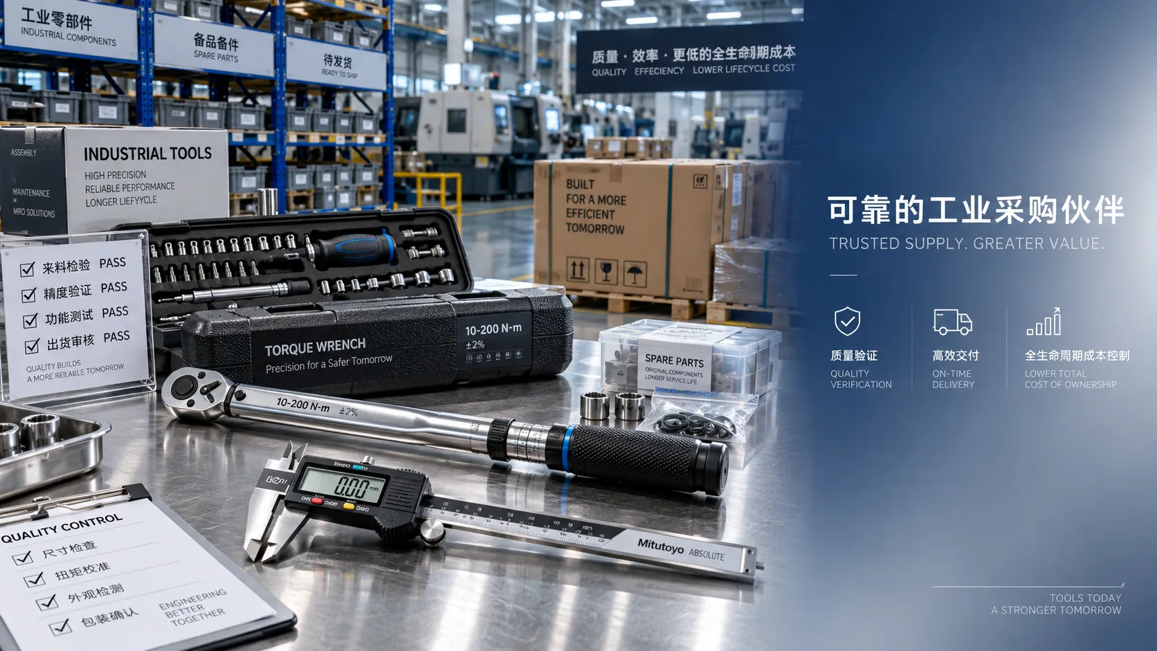
How to Compare Industrial Tool Suppliers for Quality, Lead Time, and Total Cost
Industrial tool selection supplier comparison made simple: evaluate quality, lead times, total cost, service, and supply resilience for confident sourcing decisions.
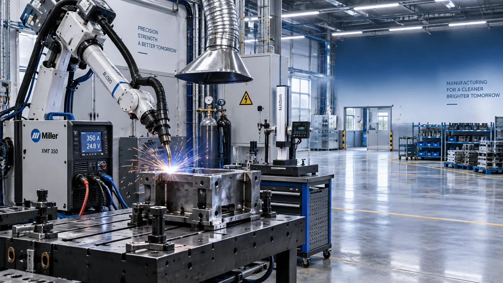
Industrial Equipment Application Guidance: Match Machines to Operating Conditions
Application guidance industrial equipment: match capacity, duty cycle, materials, site conditions, safety, and lifecycle cost to improve reliable output. Read the guide.
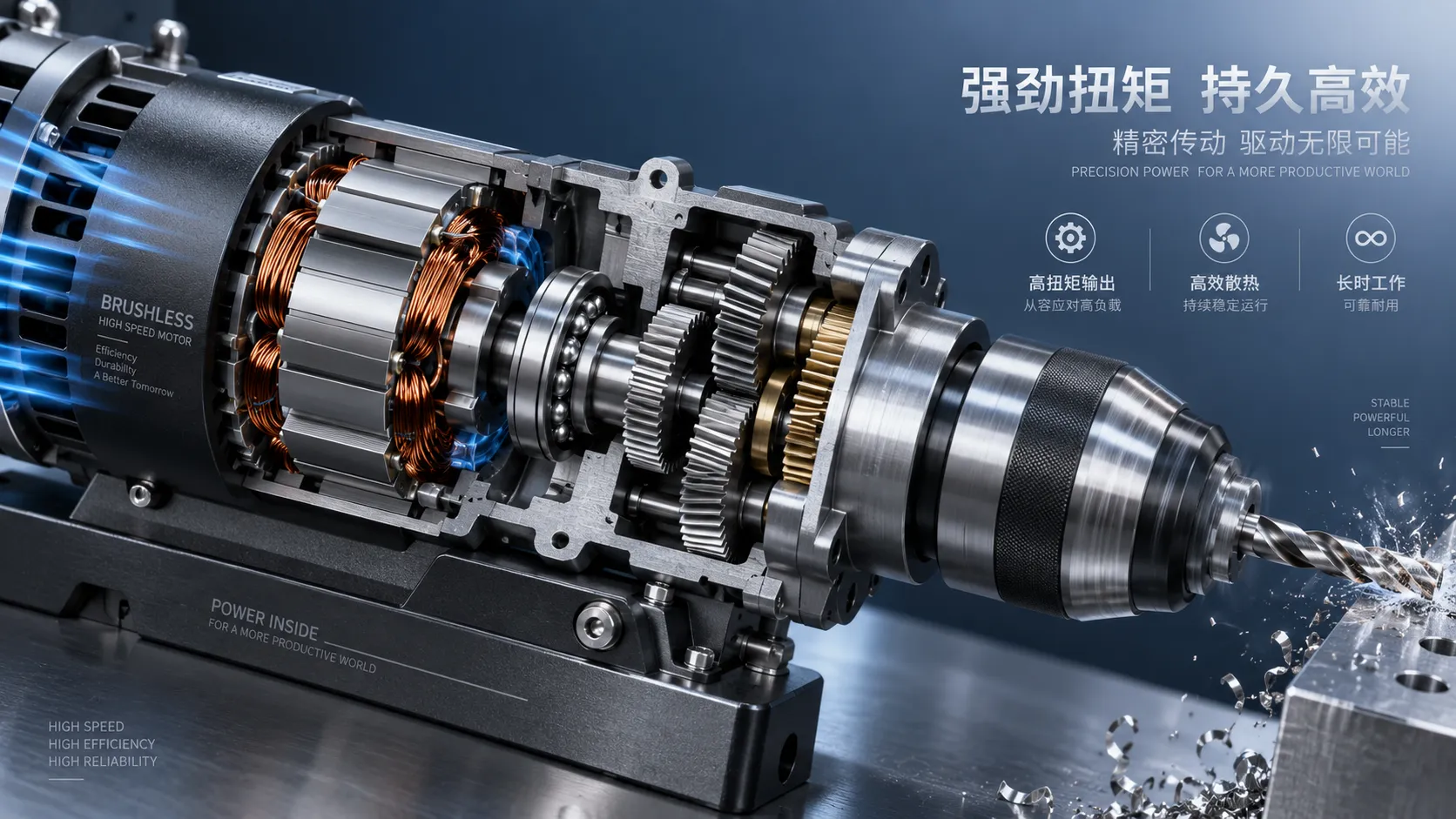
Selecting High-Speed Brushless Tool Motors for Torque, Heat, and Duty Cycle
High speed brushless tool motors: learn how to balance torque, heat, gearing, and duty cycle for reliable industrial tool performance and longer service life.
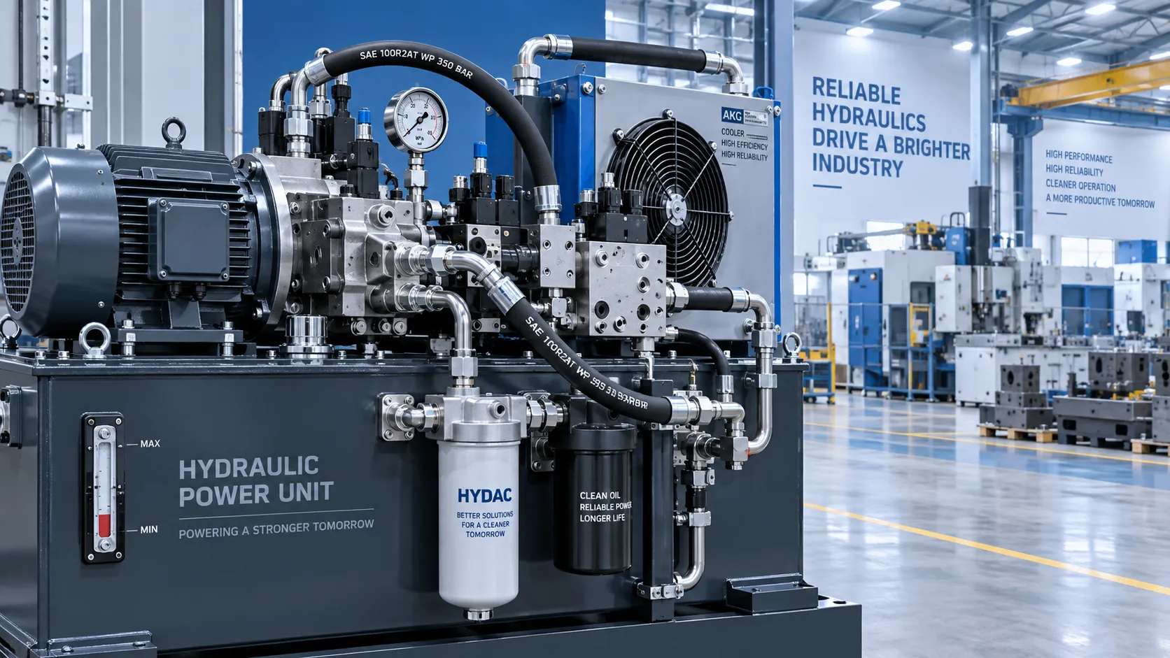
What Determines Industrial Hydraulic System Price for Heavy-Duty Equipment?
Industrial hydraulic system price depends on duty cycle, pressure, components, cooling, and integration. Compare quotes intelligently to secure reliable heavy-duty performance.
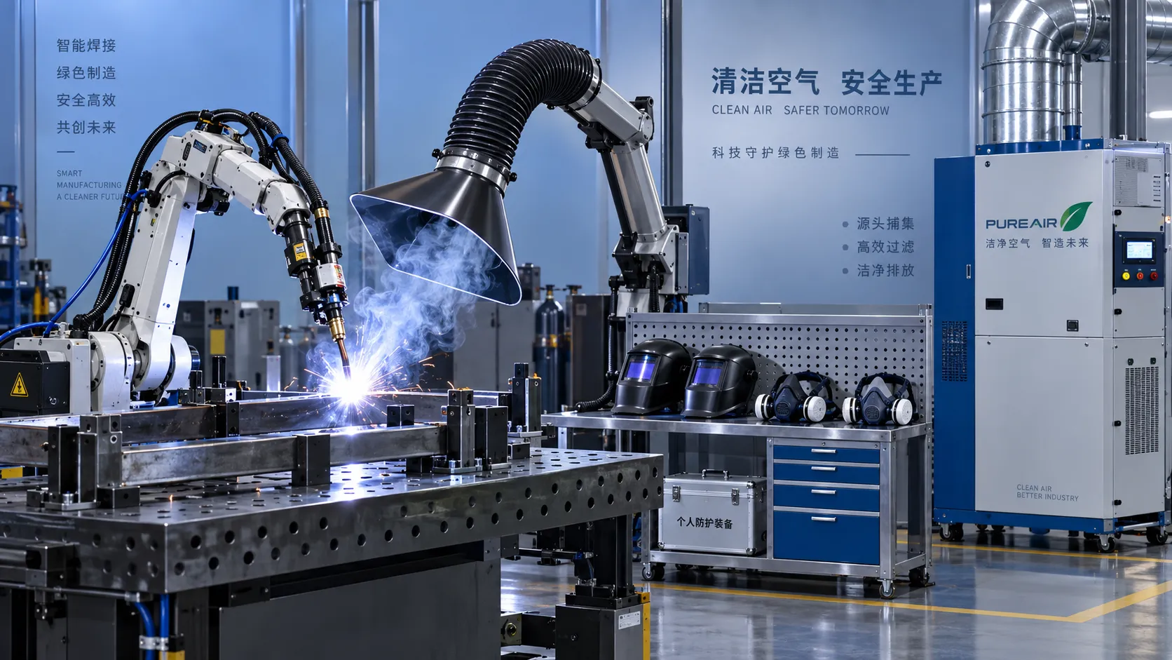
Welding Fume Extraction PPE: When Respirators Are Not Enough for Shop Safety
Welding fume extraction PPE: learn why respirators alone fall short and how source capture, ventilation, and layered controls improve shop safety.
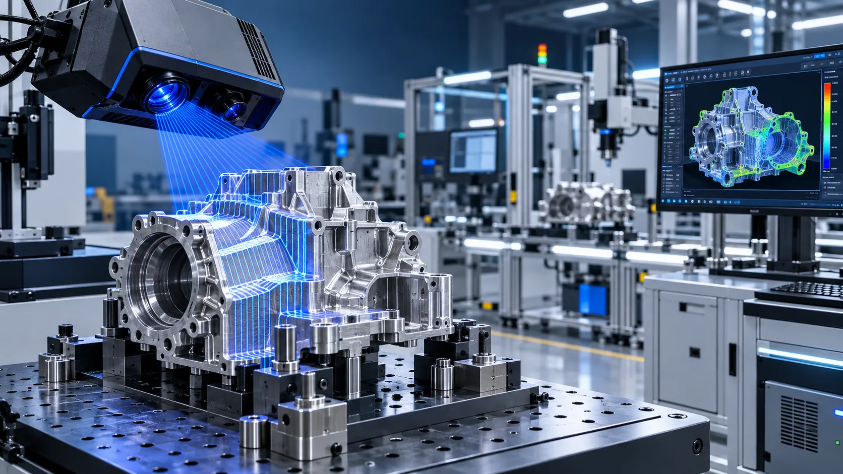
How to Select Optical Metrology Solutions for Tight-Tolerance Manufacturing
Optical industrial metrology solutions for tight-tolerance manufacturing: evaluate accuracy, surface compatibility, workflow, and traceability to select with confidence.
Related News
- 00
0000-00
Selecting Adjustable Torque Tools for Repeatable Fastener Assembly - 00
0000-00
How to Select Aerospace Inspection Tools for Aircraft Maintenance Tasks - 00
0000-00
How to Select Wire Bonding Tools for Fine-Pitch Semiconductor Packaging - 00
0000-00
Industrial Equipment Application Guidance: Match Machines to Operating Conditions - 00
0000-00
Selecting High-Speed Brushless Tool Motors for Torque, Heat, and Duty Cycle
Prof. Marcus Chen
Weekly Insights
Stay ahead with our curated technology reports delivered every Monday.